|
The use of bypass capacitors on test fixtures often is overlooked as
well as misunderstood. Time and again we find a wide variety of unusual
symptoms appearing in test environments that are found to be attributible
to Vdd fluctuations caused by unsupressed transients, rather than by some
fault of the tester. Let's look at how these transients are caused and
how they affect us even at slow test speeds.
1 MHz Scenario
In a real-world application, many events can take place in a single
1MHz cycle of 1000ns. Since different pins of the chip being tested require
different applied timing, subsequent transients can occur at corresponding
places on the 1000ns "time-line". In the list below of critical
device pins, we show "where" in time these pins experience edge
transitions, either as stimulus from the tester (as in the case of the
Clock or RESET) or as output states from the chip (Q Data, for example).
/OE = 0ns (NRZ)
CE = 50ns (NRZ)
Address [32] = 150ns (NRZ)
Q Data [32] = 700ns (Output)
Clock = 300ns and 500ns (R1)
RESET = 200ns and 600ns (RZ)
Given this fairly typical timing, the following graphical representation
can be drawn showing the timing relationships during a reset of the device.
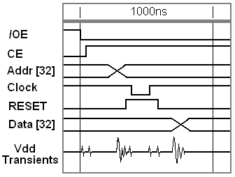
Vdd Transients induced by device switching
It can be seen in the drawing that although the test rate of this device
is 1MHz, frequencies as high as 100MHz might appear on the power pins due
to the compounded effects of node switching. Of significant interest is
the impact on Vdd of many pins switching state simultaneously, as is the
case with the 32-pin address and data busses which typically goto logic
zero at reset.
One user describes the effect and cure:
"Without a capacitor, there is a 'long' path back to the Power Supply
and there is a voltage drop across the power line. Also sense lines can
be 'slow' to react, compounding the problem. Caps create a local source
of current that can be dumped at a high rate of speed directly to the problem.
The cap speed depends on the ESR (Effective Series Resistance - effectively,
a resistor in series with the capictor). ESR values depend on the size
and type of cap. This is why there are often multiple sizes and types of
capacitors used together as one."
How Many? Where?
What we're addressing is an issue of power distribution. As designers
and test engineers can tell you, the number of ground pins needed on a
chip has a direct correlation to the number of pins that might possibly
change state simultaneously. If it is not possible to attach capacitors
to all power pins, place them on (at least) the power pins sourcing
those I/O pins that are most likely to change state/direction in unison.
Such pins might be data or address busses that "zero out" during
a reset or an address rollover. Making this determination may require intimate
knowledge of the chip's substrate structure.
|
Bypass Capacitors
You will need .001, .01 and .1 uf bypass capacitors positioned right
at the power pins of the DUT chip socket for a local reservoir of power.
Keep the leads as short as possible, and No Electrolytics! The farther
your DUT is from the capacitors, the less effective the capacitors are.
Electrolytics can store power long after the test is completed, causing
problems during subsequent continuity tests or when the test is a Production
situation; the device may still be "powered" when the handler
steps to the next chip. The different capacitor values and types (mylar,
ceramic, etc.) serve to provide appropriate characteistics depending on
the transient frequencies involved. As we've already seen, many frequencies
may be present regardless of the test rate used.
'Scope it out
To view your Vdd on an oscilloscope follow these steps:
- Define a new group in the Pin Setup window as "Trig"
for the scope trigger. Put an unused tester channel in this group and call
it "trig", display in binary. Set direction to DUT Input, NRZ
data format, Leading edge 0ns.
- Select a scope channel other than channel one as the trigger
source, and connect the probe for that channel to the "trig"
ETS channel on the DUT board. Set the trigger for a positive (rising) edge
trigger. Connect channel one of the scope to a Vdd+ pin on the chip, close
to the body.
- Edit the data in the Vectors window. Fill the "trig"
pin with logic 0 for the entire vector set by pulling down the "Vectors"
drawer at the top of the screen. Locate the desired vector at which the
greatest number of node state changes is taking place, such as the RESET
in our example. Place a logic 1 on the "trig" pin at this vector.
- Prepare to execute by setting the Stop Condition in the Run
Setup window to "NONE". All of the vectors will be executed up
to the Last Vector defined on this window. If using the Programmed mode,
you must put a JMP at the Last Vector returning to the start of the vectors.
- Power should be defined in the DUT Power window before running.
When RUN button is clicked, the tester will cycle endlessly through the
vectors until the stop sign is clicked. As it runs, the scope can be fine
tuned to display the Vdd condition at the selected vector.
Conclusion
If you've done without capacitors in the past, reconsider your practices.
Odd behavior you may recall from earlier test efforts may lead you to suspect
poor power management that could have been avoided with better fixturing
discipline.
Related info
Q'nApp #L9: Iddq Testing
Q'nApp #L20: Power and Ground
QL22.zip is a zipped Word file of this Q'nApp.
Click your browser's Back button to return to
the Q'nApps
index.
|